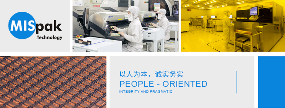
MISpak technology Co., Ltd., as one of the largest suppliers of MIS packaging material in the world,specializes in MIS packaging materials development, production and sales services and provide MIS package solutions based on customer requirements.
Our MIS productshas the combined advantage of both the assembly leadframe and organic substrate, to realize the packaging needs of high density I/O, multi-row QFN, BGA, MCM, MIS-SiP and MIS-3D. With the superior advantages of higher routing density, better electrical and thermal performance, possible to integrate with multi-functional components, MIS is widely used in various electrical application fields, such as power management products, touch panel products, wearable products, wireless chargeable products and so on. Apparently, it meets the increasing packaging requirements of high density, high performance and multi-function.
In the course of our MIS product development, we have come up with numerous solutions for our customers, making contributions to the development of the semiconductor industry. Our efforts have been recognized by the peer industry. In March 2014,we won the Award for Contribution to the Industry from SemiChina, and the Award for Technological Innovation of China's Semiconductor Association.
We will persistently pursue higher product quality and better customer service and strengthen technical innovation, to create value added for our customers.


